
Jetson GPIO Pin Write
Writes a value of a trigger condition to a GPIO pin.
Overview
Writes to GPIO pins on Jetson devices.
Inputs & Outputs
- Inputs : 1, Media Format : Any
- Outputs : 1, Media Format: Same as Input
- Output Metadata : None
Properties
| Property | Description | Type | Default | Required |
|---|---|---|---|---|
gpio_pin_name | Comma separated list of GPIO pin names in the kernel naming scheme. The pins will be configured to be writable in the OUT direction. | string | null | Yes |
trigger | Trigger Condition whose result is to be written to the chosen GPIO pin. | trigger-condition | null | Yes |
mode | Write mode. Options: Write on change (pulse) (pulse); Write on every frame (hold) (hold). | enum | pulse | Yes |
activity | Activity. Options: Active high (high): For raw wire signal; Active low (low): For pins with inverted logic. | enum | high | Yes |
PIN Names
This node refers to pins using their kernel-assigned names, e.g. PQ.01, PAA.16, etc.
AIMobile
AIMobile Jetson Xavier NX (NCX1), Orin Nano and NX (NCON, NCOX)
For the AI Mobile Orin devices, there two exposed DIO pin that can be configured in OUT direction on the xcon devices (Orin Nano 4/8GB, Orin NX 8/16GB). The pin mapping is below.
| Pin Identifier | GPIO Pin Name (use in Node) |
|---|---|
| GPIO1 (see image below). | PQ.05 |
| GPIO2 (see image below). | PQ.06 |
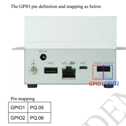
GPIO1 and GPIO2 are the two GPIO pins available on AIMobile devices.
AIMobile Orin Multi-IO Devices (PSOX, PSON)
| PIN Identifier (see image below) | GPIO Pin Name | Notes |
|---|---|---|
| DI1 | PZ.03 | Input Only |
| DI2 | PZ.04 | Input Only |
| DI3 | PZ.05 | Input Only |
| DI4 | PZ.06 | Input Only |
| DO1 | PY.00 | Output Only |
| DO2 | PY.01 | Output Only |
| DO3 | PY.02 | Output Only |
| DO4 | PY.03 | Output Only |
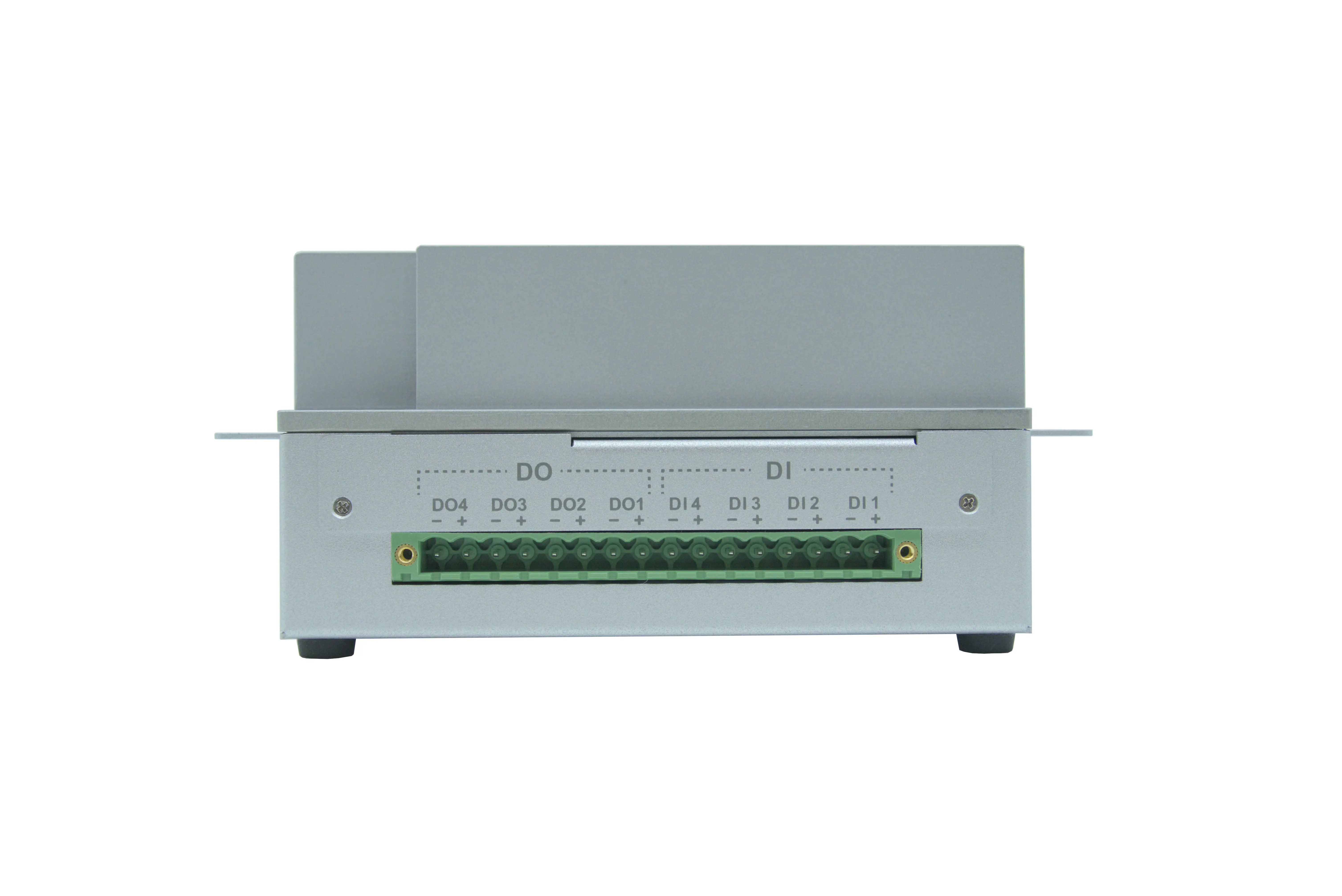
DI 1-4 and DO 1-4 are the pins exposed on the PSON and PSOX devices.
Aaeon
Aaeon Boxer 8652AI
For the Aaeon Boxer 6852AI - Orin devices, there 13 exposed DIO pin that can be configured. The pin mapping is below.
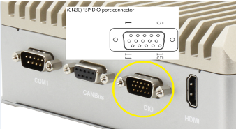
CN30 connector. Pins numbered 1 through 15, starting from top left.
| PIN Identifier | GPIO Pin Name (use in Node) | Function |
|---|---|---|
| 1 | - | VDD_3V.3_SYS |
| 2 | PY.02 | 37P_SPI1_MOSI_LS |
| 3 | PY.01 | 22P_SPI1_MISO_LS |
| 4 | PY.00 | 13P_SPI1_SCK_LS |
| 5 | PY.03 | 18P_SPI1_CS0_LS |
| 6 | PZ.05 | 19P_SPI0_MOSI_LS |
| 7 | PZ.04 | 21P_SPI0_MISO_LS |
| 8 | PZ.03 | 23P_SPI0_SCK_LS |
| 9 | PZ.06 | 24P_SPI0_CS0_LS |
| 10 | PZ.07 | 26P_SPI0_CS1_LS |
| 11 | PI.02 | 35P_I2S0_LRCK_LS |
| 12 | PI.01 | 38P_I2S0_SDIN_LS |
| 13 | PI.00 | 40P_I2S0_SDOUT_LS |
| 14 | PH.07 | 12P_I2S0_SCLK_LS |
| 15 | - | GND |
Output Metadata
Node does not insert any output metadata; upstream metadata continues through the pipeline
Updated 3 months ago